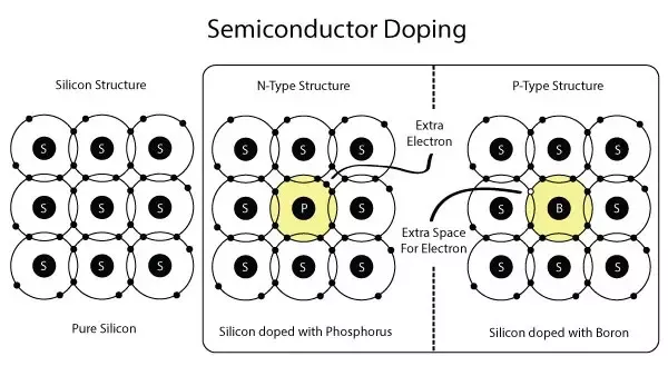
What is Doping Process?
Doping
Doping is the process in which impurities are added to a semiconductor to change/control it’s electrical properties. The semiconductor in which impurities are added is called extrinsic semiconductor.
Doping is done in semiconductors for three main reasons:
* Change the conductivity of the material.
* To produce junctions.
* Doping increases the electrical conductivity of a semiconductor.
Process of Doping
Simple P-N junction diode can be made by doping pentavalent or donor impurity in one portion and trivalent or acceptor impurity in other portions of silicon or germanium crystal block. This doping makes a PN junction at the middle part of the block. We can also form a PN junction by joining a p-type and n-type semiconductor together with a special fabrication technique. Dopant is integrated into a lattice structure where the number of outer electrons defines the type of doping. Elements with 3 valence electrons are used for p-type doping while 5 valence electrons are used for n-type doping. There is a free electron with n-type doping and can be moved into the conduction band with little energy as it is not bound. For a p-type doping, there is a free hole for acceptor energy level band.
EXAMPLE
Silicon in an un-doped state is non conductive as it creates covalent bonds with itself resulting in essentially no free electrons to make the circuit work. When an impurity e.g. phosphorus is added to provide those free electrons to move around the circuit, the process is called doping or implantation of the silicon.
It is done in three steps:
1. Pattern the area to be doped.
2. Implant the dopant (such as phosphorus). This is done by shooting the dopant at the surface of the semiconductor using an ion implanter which simplistically is an ion source accelerated by an electromagnet.
3. Diffuse the dopant into the silicon. This is done using extremely high heat.We can consider the second step as adding butter to a toast and the third step as the butter is melting into the toast.
N-TYPE MATERIAL
A n-type semiconductor is characterized as a type of extrinsic semiconductor doped with a pentavalent impurity element that has five electrons in its valence shell. In the n-type semiconductor the pentavalent impurity or dopant elements are added to increase the number of electrons for conduction.
P-TYPE MATERIAL
A p-type semiconductor has more holes than electrons. This allows the current to flow along the material from hole to hole but only in one direction. P-type semiconductors are created by doping an intrinsic semiconductor with an electron acceptor element. One common p-type silicon dopant is boron or gallium.
Making PN Junction Diode
P-n junctions are created by joining n-type and p-type semiconductor materials. Since the area of n-type has a higher concentration of electrons and the p-type has a higher concentration of holes, electrons migrate from the n-type side to the p-type side. Simultaneously, holes flow from the p-type side to the n-type side by diffusion.
The free electrons diffusing into the p-type region from the n-type region would recombine with holes available there and create uncovered negative ions in the p-type region. In the same way, the holes diffusing into the n-type region from the p-type region would recombine with free electrons available there and create uncovered positive ions in the n-type region.
When the electrons and holes move to the other side of the junction at a p-n junction, they leave behind exposed charges on dopant atom sites fixed in the crystal lattice and unable to move. Positive ions are exposed on the n-type side and negative ions are exposed on the p-type side. An electric field E is formed between the positive ion cores in the material of n-type and the negative ion cores in the material of p-type. This region is called "Depletion region."

