Introduction to diode
What is Diode:
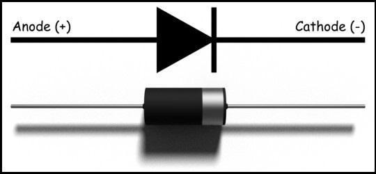
A Diode is defined as a two-terminal electronic component that only conducts current in one direction (as long as it is operated within a specified voltage level). An ideal diode will have zero resistance in one direction, and infinite resistance in the reverse direction. It’s an important part of any electrical or electronics circuit and none of the circuits are complete without the usage of diodes. Its analogy is the same as the purpose of a valve in air or water flows. Its symbol is mentioned in the picture. The arrowhead represents conventional current flow in the forward biased condition. Its two terminals are called Anode and Cathode, where anode is shown as a “Positive mark” and cathode is shown as a “Negative mark.”
Working Principle of Diode:
A diode’s working principle depends on the interaction of n-type and p-type semiconductors. An n-type semiconductor has plenty of free electrons and a very few numbers of holes. In other words, the concentration of free electrons is high. Free electrons in the n-type semiconductor are referred to as majority charge carriers, and holes in the P-type semiconductor are referred to as minority charge carriers. Contrary to N-type, a P-type semiconductor has a high concentration of holes and a low concentration of free electrons. Holes in the p-type semiconductor are majority charge carriers, and free electrons in the p-type semiconductor are minority charge carriers. Diodes begin conducting electricity only if a certain threshold voltage is applied in the forward direction (i.e. the "low resistance" direction), hence called forward-biased. When a diode is connected in the reverse direction it means that the diode is reversed biased (i.e. the "high resistance" direction).
There are two types of Diode operations:
Forward Biased
In the case of forward-based diode operations where a source's positive terminal is connected to the p-type side and the source's negative terminal is connected to the diode's n-type side, and one can gradually increase the source's voltage from zero. At first, there is no current that flows through the diode. The depletion region is considered to serve as a potential barrier against the majority-charge carriers known as forward potential barriers. The majority of charge carriers only begin to cross the forward potential barrier when the value of the externally applied voltage across the junction is greater than the forward barrier potential. The forward barrier potential is 0.7 volts for silicone diodes and 0.3 volts for germanium diodes. Once the forward voltage applied externally through the diode is greater than the forward barrier potential, the free majority charge carriers begin to cross the barrier and contribute towards the forward diode current. The diode will act as a short-circuited path in that case, and the forward current is confined to the diode only by externally attached resistors.
Reverse Biased
In reverse biased mode, we connect the voltage source's negative terminal to the p-type side, and the voltage source's positive terminal to the n-type side of the diode. Due to the electrostatic attraction of the source's negative potential, the p-type region's holes will be moved further from the junction, leaving more exposed negative ions at the junction. Similarly, the free electrons in the n-type region will be moved further away from the junction to the positive voltage source terminal leaving further positive ions at the junction. The depletion region becomes wider as a result of this phenomenon. This diode condition is called the reverse biased state. No majority carriers cross the junction at that point, and then they shift away from the junction. In this way, a diode blocks current flow when it is reverse biased, so that the current is transmitted in one direction only (as long as it is regulated within a defined voltage level).

